- 您现在的位置:买卖IC网 > Sheet目录406 > DMN3112SSS-13 (Diodes Inc)MOSFET N-CH 30V 6A 8SOP
�� �
�
�DMN3112SSS�
�SINGLE� N-CHANNEL� ENHANCEMENT� MODE� MOSFET�
�Product� Summary�
�Features� and� Benefits�
�V� (BR)DSS�
�30V�
�R� DS(ON)� max�
�57m� ?� @� V� GS� =� 10V�
�112m� ?� @� V� GS� =� 4.5V�
�I� D� max�
�T� A� =� +25°C�
�6.0A�
�3.8A�
�?�
�?�
�?�
�?�
�?�
�?�
�Low� On-Resistance�
�Low� Gate� Threshold� Voltage�
�Low� Input� Capacitance�
�Fast� Switching� Speed�
�Low� Input/Output� Leakage�
�Totally� Lead-Free� &� Fully� RoHS� Compliant� (Notes� 1� &� 2)�
�?�
�?�
�Halogen� and� Antimony� Free.� “Green”� Device� (Note� 3)�
�Qualified� to� AEC-Q101� Standards� for� High� Reliability�
�Description� and� Applications�
�Mechanical� Data�
�This� MOSFET� has� been� designed� to� minimize� the� on-state�
�resistance� (R� DS(on)� )� and� yet� maintain� superior� switching�
�performance,� making� it� ideal� for� high� efficiency� power� management�
�applications.�
�?� Backlighting�
�?� Power� Management� Functions�
�?� DC-DC� Converters�
�?�
�?�
�?�
�?�
�?�
�?�
�Case:� SOP-8L�
�Case� Material:� Molded� Plastic,� “Green”� Molding� Compound.�
�UL� Flammability� Classification� Rating� 94V-0�
�Moisture� Sensitivity:� Level� 1� per� J-STD-020D�
�Terminals� Connections:� See� Diagram�
�Terminals:� Finish� -� Matte� Tin� annealed� over� Copper� lead�
�frame.� Solderable� per� MIL-STD-202,� Method� 208�
�Weight:� 0.074g� (approximate)�
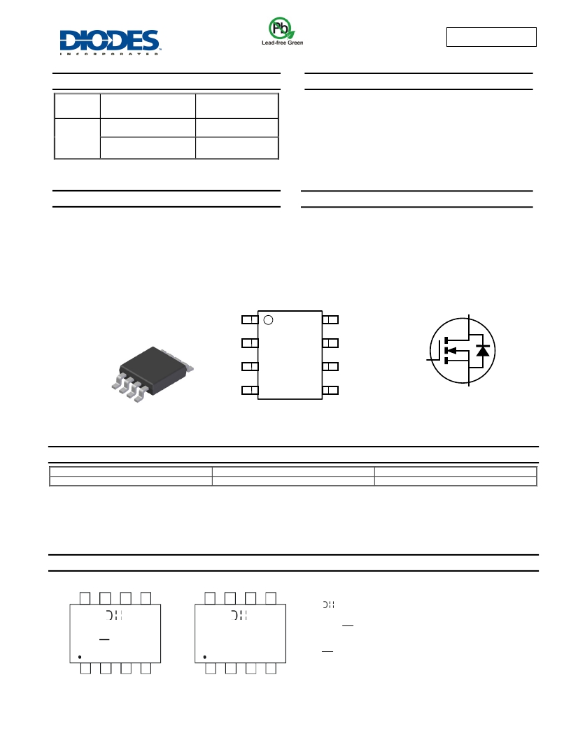
�SOP-8L�
�S�
�S�
�D�
�D�
�D�
�TOP� VIEW�
�Ordering� Information�
�(Note� 4)�
�Part� Number�
�DMN3112SSS-13�
�S�
�G�
�Top� View�
�Internal� Schematic�
�Case�
�SOP-8L�
�D�
�D�
�G�
�S�
�Equivalent� circuit�
�Packaging�
�2500/Tape� &� Reel�
�Notes:�
�1.� No� purposely� added� lead.� Fully� EU� Directive� 2002/95/EC� (RoHS)� &� 2011/65/EU� (RoHS� 2)� compliant.�
�2.� See� http://www.diodes.com/quality/lead_free.html� for� more� information� about� Diodes� Incorporated’s� definitions� of� Halogen-� and� Antimony-free,� "Green"�
�and� Lead-free.� ?�
�3.� Halogen-� and� Antimony-free� "Green”� products� are� defined� as� those� which� contain� <900ppm� bromine,� <900ppm� chlorine� (<1500ppm� total� Br� +� Cl)� and�
�<1000ppm� antimony� compounds.�
�4.� For� packaging� details,� go� to� our� website� at� http://www.diodes.com/products/packages.html.�
�Marking� Information�
�8�
�5�
�8�
�5�
�=� Manufacturer’s� Marking�
�N3112SS� =� Product� Type� Marking� Code�
�YYWW� =� Date� Code� Marking�
�N3112SS�
�YY� WW�
�N3112SS�
�YY� WW�
�YY� or� YY� =� Year� (ex:� 13� =� 2013)�
�WW� =� Week� (01� -� 53)�
�YY� =� Date� Code� Marking� for� SAT� (Shanghai� Assembly/� Test� site)�
�YY� =� Date� Code� Marking� for� CAT� (Chengdu� Assembly/� Test� site)�
�1�
�4�
�1�
�4�
�Chengdu� A/T� Site�
�Shanghai� A/T� Site�
�DMN3112SSS�
�Document� number:� DS31582� Rev.� 2� -� 2�
�1� of� 5�
�www.diodes.com�
�October� 2013�
�?� Diodes� Incorporated�
�发布紧急采购,3分钟左右您将得到回复。
相关PDF资料
DMN3115UDM-7
MOSFET N-CH 30V 3.2A SOT-26
DMN3135LVT-7
MOSFET N CH 30V 4.1A TSOT26
DMN3150L-7
MOSFET N-CH 28V 3.2A SOT23-3
DMN3150LW-7
MOSFET N-CH 28V 1.6A SC70-3
DMN3200U-7
MOSFET N-CH 30V 2.2A SOT23-3
DMN32D2LDF-7
MOSFET 2N-CH 30V 400MA SOT353
DMN32D2LFB4-7
MOSFET N-CH 30V 300MA 3-DFN
DMN32D2LV-7
MOSFET N-CH DUAL 30V SOT-563
相关代理商/技术参数
DMN3115UDM
制造商:Diodes Incorporated 功能描述:MOSFET N CH W ESD 30V 3.2A SOT26 制造商:Diodes Incorporated 功能描述:MOSFET, N CH, W ESD, 30V, 3.2A, SOT26
DMN3115UDM-7
功能描述:MOSFET 900mW 30Vdss RoHS:否 制造商:STMicroelectronics 晶体管极性:N-Channel 汲极/源极击穿电压:650 V 闸/源击穿电压:25 V 漏极连续电流:130 A 电阻汲极/源极 RDS(导通):0.014 Ohms 配置:Single 最大工作温度: 安装风格:Through Hole 封装 / 箱体:Max247 封装:Tube
DMN3135LVT-7
功能描述:MOSFET MOSFET BVDSS: 31V-40 1V-40V TSOT23 T&R 3K RoHS:否 制造商:STMicroelectronics 晶体管极性:N-Channel 汲极/源极击穿电压:650 V 闸/源击穿电压:25 V 漏极连续电流:130 A 电阻汲极/源极 RDS(导通):0.014 Ohms 配置:Single 最大工作温度: 安装风格:Through Hole 封装 / 箱体:Max247 封装:Tube
DMN3150L
制造商:DIODES 制造商全称:Diodes Incorporated 功能描述:N-CHANNEL ENHANCEMENT MODE FIELD EFFECT TRANSISTOR
DMN3150L-7
功能描述:MOSFET N-Channel RoHS:否 制造商:STMicroelectronics 晶体管极性:N-Channel 汲极/源极击穿电压:650 V 闸/源击穿电压:25 V 漏极连续电流:130 A 电阻汲极/源极 RDS(导通):0.014 Ohms 配置:Single 最大工作温度: 安装风格:Through Hole 封装 / 箱体:Max247 封装:Tube
DMN3150LW
制造商:DIODES 制造商全称:Diodes Incorporated 功能描述:N-CHANNEL ENHANCEMENT MODE FIELD EFFECT TRANSISTOR
DMN3150LW-7
功能描述:MOSFET 0.35W 28V 1.6A RoHS:否 制造商:STMicroelectronics 晶体管极性:N-Channel 汲极/源极击穿电压:650 V 闸/源击穿电压:25 V 漏极连续电流:130 A 电阻汲极/源极 RDS(导通):0.014 Ohms 配置:Single 最大工作温度: 安装风格:Through Hole 封装 / 箱体:Max247 封装:Tube
DMN3200U
制造商:DIODES 制造商全称:Diodes Incorporated 功能描述:N-CHANNEL ENHANCEMENT MODE FIELD EFFECT TRANSISTOR